
V-by-One® HS IP Standard Interface
High-Speed Video Serial Interface Compliant with the V-by-One HS Standard
V-by-One HS is a standard for next-generation high-speed interface technology developed by THine Electronics for image and video equipment requiring higher frame rates and higher resolutions. Implementing the V-by-One HS Standard Interface in Altera FPGAs reduces the number of signals compared with conventional LVDS interfaces, which greatly reduces product cost.
Features
- V-by-One HS Standard Interface achieves 4 Gbps maximum transmission rate per lane (actual rate depends on the FPGA device)
- Supports custom video formats as well as VESA, SMPTE, and other standard formats
- Supports flexible multi-lane designs in accordance with the user's total transmission rate requirement
- Self-check function (FieldBET) to test connectivity between transmitter and receiver IP
Specifications
| Transmitter IP | Receiver IP | |
|---|---|---|
| Lane | 1~32 | |
| Pixel Data | 24,32,40 bit | |
| Self Test Function | FieldBET Pattern Generator | FieldBET PatternChecker |
Supported Devices
- Cyclone® V GX/SX/GT/ST, Cyclone® 10 GX
- Arria® V GX/SX/GT/ST/GZ, Arria® 10 GX/SX
- Stratix® V GX, Stratix® 10 GX/SX (L/H-Tile)
- Agilex® 5E (Group B)
Please contact your local Macnica sales representative or use our contact form for information about other devices.
Deliverables
- Encrypted RTL (Verilog HDL)
- Reference design
- Simulation environment (For ModelSim)
- User's manual
- Reference design user's guide
Device Resource Utilization
| IP | Lane | Cyclone IV GX | Arria II GX | Stratix IV GX | ||||||
| LE | Register | Block Memory | ALUT | Register | Block Memory | ALUT | Register | Block Memory | ||
|---|---|---|---|---|---|---|---|---|---|---|
| TX | 2 | 3946 | 2782 | 0 | 1933 | 2782 | 0 | 1933 | 2782 | 0 |
| RX | 2 | 6477 | 4949 | 0 | 2574 | 4949 | 0 | 2574 | 4949 | 0 |
| IP | Lane | Cyclone V GX | Arria V GX | Stratix V GX | Arria 10 GX | ||||||||
| LE | Register | Block Memory | ALUT | Register | Block Memory | ALUT | Register | Block Memory | ALUT | Register | Block Memory | ||
|---|---|---|---|---|---|---|---|---|---|---|---|---|---|
| TX | 2 | 1598 | 2977 | 0 | 1603 | 2964 | 0 | 1635 | 2959 | 0 | 1674 | 2976 | 0 |
| RX | 2 | 2273 | 5416 | 0 | 2274 | 5377 | 0 | 2259 | 5351 | 0 | 2528 | 5218 | 0 |
* The values in the above table are based on an example implementation. There may be some variation depending on the user’s system configuration.
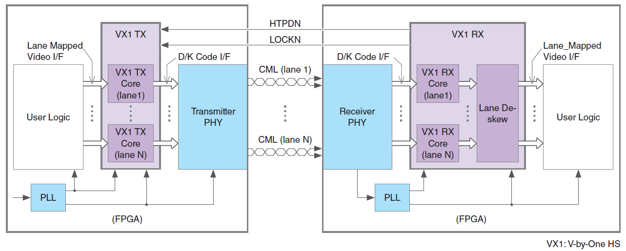
Configuration Diagram
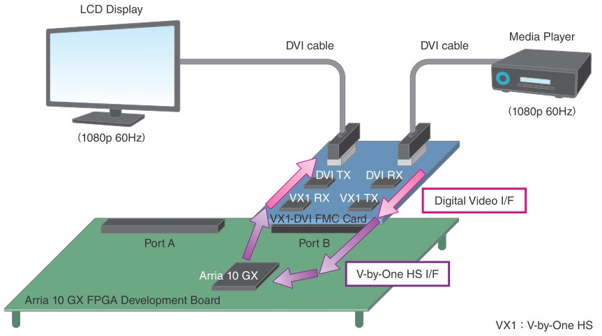
Evaluation Environment
| Product Name | Vendor | |
|---|---|---|
| Main Board | Arria 10 GX FPGA Development Board | Terasic |
| Daughter Card | V-by-One HS DVI FMC Card | Mpression |
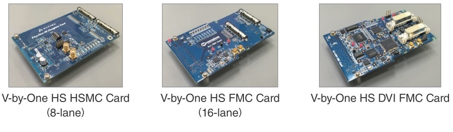
Evaluation Boards
Resources
Macnica Americas Site Map


©Copyright 2026 Macnica Americas, Inc.